|
SINGLE DISC ELECTRODESTM
(SDEs) |
|
|
|
|
|
|
|

|
MDEA DEVICES |
Number of Discs |
Disc dimensions |
Active Area |
Conductor |
|
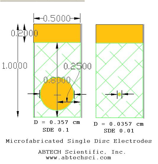
SDE Au 0.1 |
1 disc |
0.357 cm diameter |
0.10 cm2 |
Au |
|
SDE Au 0.01 |
1 disc |
0.036 cm diameter |
0.01 cm2 |
Au |
|
SDE Pt 0.1 |
1 disc |
0.357 cm diameter |
0.10 cm2 |
Pt |
|
SDE Pt 0.01 |
1 disc |
0.036 cm diameter |
0.01 cm2 |
Pt |
|
|
|
|
|
|
SDE Brochure (PDF) |
|||||
|
|||||||||
|
Ø Chip Substrate: |
Schott D263 Borosilicate Glass |
|
|||||||
|
|
Dielectric Constant, Epsilon(r) at 1 MHz |
6.7 |
|||||||
|
|
Dielectric Loss Angle, tan delta, at 1 MHz |
61 x 10-4 |
|||||||
|
|
Electrical Resistivity (50 Hz) (250 C) |
1.6 x 10^8 ohm cm |
|||||||
|
|
Coefficient of Linear Thermal Expansion, * 20-300 Deg C |
7.2 x 10^-6 K^-1 |
|||||||
|
|
Refractive Index at 20 C, ne ( Lambda = 546.1 nm) |
1.5249 |
|||||||
|
|
|
|
|||||||
|
Ø Metallization: |
100 Å Ti|W / 1000 Å Au or Pt and ITO = 10 Ohms/sq |
|
|||||||
|
|
|
|
|||||||
|
Ø Insulating Top Layer: |
Silicon Nitride (Si3N4) |
|
|||||||
|
|
|
|
|||||||
|
|
|
No of Discs |
Electroactive Area (cm2) |
Geometric Area (cm2) |
|||||
|
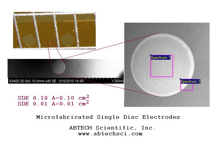
Ø SDE 0.10 |
A single disc, 0.357 cm diameter. |
1 |
1.0 x10⁻¹ |
1.0 x10⁻¹ |
|||||
|
Ø SDE 0.01 |
A single disc, 0.0357 cm diameter |
1 |
1.0 x10⁻² |
1.0 x10⁻² |
|||||
|
|
|
|
|
|
|||||
|
Ø SDE Chip Dimensions |
Un-packaged Die |
Packaged Die |
|||||||
|
|
(l x w x t) |
(l x w x t) |
|||||||
|
SDE X.XX |
1.00 x 0.50 x 0.05 cm |
N.A. |
|||||||
|
|
|
|
|||||||
|
Ø Packaging |
|
|
|||||||
|
Electrode Body: |
N.A. |
||||||||
|
Encapsulant: |
N.A. |
||||||||
|
Leadwires: |
N.A. |
||||||||
Back to Index |
|||||||||